
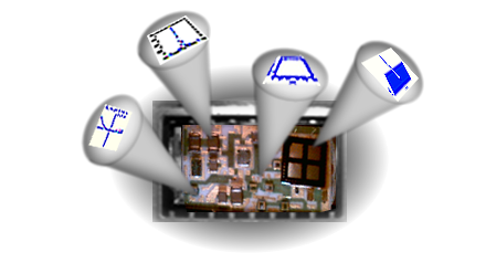

Product Characterization
The emerging nature of microsystems, the multi-domain nature of the physics involved, and the initial small production volumes determine that microsystems characterization and testing are not as advanced as in other related fields. The back-end QA processes contribute a significant part of the cost and are a common cause of project delays due to unavailability of appropriate tools. Device testing often requires one-of-a-kind instruments or unique suites of diagnostic tools for measuring the electrical, mechanical, and optical characteristics of devices and systems. Microsystems can also require specialized non-contact characterization and testing methodologies.
Our company is offering, as part of our Package-CentricSM microsystem engineering service, a suite of proven design techniques for making device characterization easier using off-the-shelf or semi-custom equipment. We have also developed efficient testing protocols for characterizing and testing devices. We have developed procedures for optimally using known-good-die integrated circuits for on-board system control, methods for passive or active fiber positioning and alignment, and techniques for controlling the packaged device internal environment.
We are also experienced in developing unique MEMS/MST device characterization solutions, such as automated non-contact wafer level inspection systems for post-release device characterization.